Solved i need help turning this circuit into kicad pcb, i Kicad update schematic from pcb Kicad generate pcb from schematic
Solved I need help turning this circuit into KiCAD PCB, I | Chegg.com
Pcb kicad daumemo Design and modify pcb and schematic in kicad by zunuran1 Design a pcb for the very first time in kicad : 9 steps (with pictures
Kicad update schematic from pcb
Kicad tutorial board tutorials source open pcb schematic editor simple store choose valuable fundamentals layoutKicad schematic and pcb Design a pcb for the very first time in kicad : 9 steps (with picturesHow to create your first kicad pcb project?.
Creating a pcb in everything: kicad, part 1How do i convert a schematic to pcb layout in kicad ? – pcb hero Make your kicad schematic, pcb layout, and production files by mohamedHow do i convert a schematic to pcb layout in kicad (step by step).

Kicad pcb hackaday nanite wesley
Pcb designing part 1: how to design the schematics (kicad)Kicad pcb schematic example Tutorials for kicad-an open source schematic / pcb editorDesign a pcb for the very first time in kicad : 9 steps (with pictures.
Kicad pcb schematic creating everything part hackaday completed board ourHow to create your first kicad pcb project? Design schematic and pcb layout in kicad by tikmapPcb kicad daumemo.

Let the experts talk about : does kicad provides cross probe between
Make this into kicad, and provide schematic and pcbThe best pcb design and schematic using altium , kicad or easy eda Design a pcb for the very first time in kicad : 9 steps (with picturesKicad pcb schematics.
Intro to pcb design part 2 // designing your schematic with kicad 4.0Arduino uno kicad pcb circuits Kicad pcb schematic component footprints assign select tools menu firstDesigning pcbs with kicad.

Schematic to pcb in kicad
Convert a schematic drawing to pcb using kicad : reverse engineering aDesign a pcb for the very first time in kicad : 9 steps (with pictures Get from schematic to pcb fasterKicad how to: turning your pcb into reality.
Creating a pcb in everything: kicad, part 2Comenzando en kicad How to convert schematic to pcb layout in kicad.


Intro to PCB Design Part 2 // Designing Your Schematic with KiCad 4.0

How to create your first KiCAD PCB project? - Daumemo

Documentation | KiCad
Comenzando en KiCad | 7.0 | Español | Documentation | KiCad

How do I convert a Schematic to PCB Layout in KiCad ? – PCB HERO

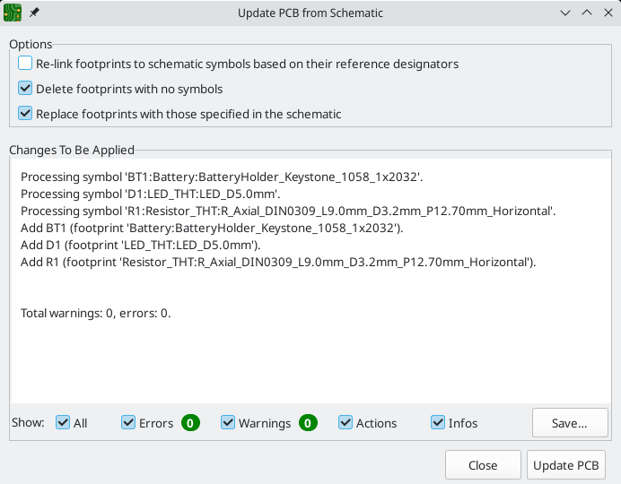
Kicad Update Schematic From Pcb

Tutorials for KiCad-an Open Source Schematic / PCB Editor - Curious

The best PCB design and schematic using Altium , KiCAD or Easy EDA | Upwork
